Electronics
Improve Process Times, Increase Process Yields
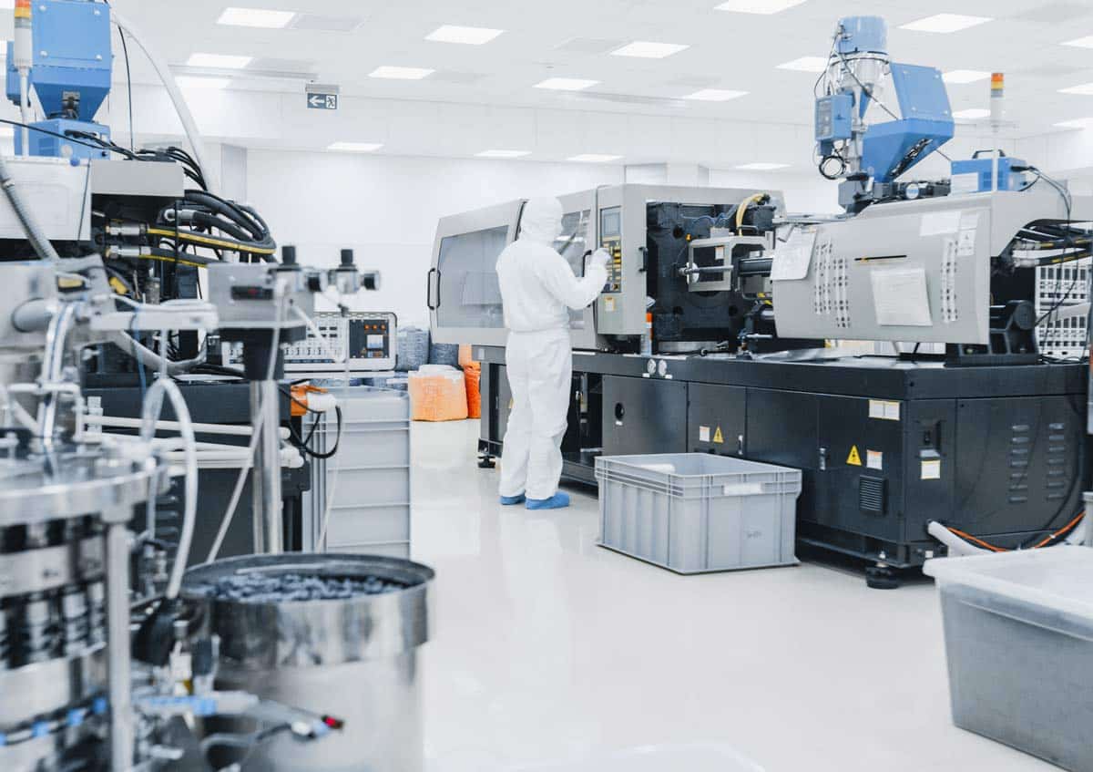
Mass production of electronics requires knowledge of industry process, quality requirements and yield expectations, as well as specialized expertise in the processing of challenging materials. From any variety of glass to hard ceramics, handling, cutting, surface treatments, milling, and more, our in-depth know-how at Shape Process Automation becomes our customer’s competitive advantage. Whether your manufacturing is high-mix/low-volume or low-mix/high-volume, our flexible automation solutions mean you get the right equipment with the right process to match your specific needs – all while driving down costs by eliminating unnecessary resources and process inefficiencies.
We work with industry leaders to create processes for highly technical, high end-electronics, improving and automating overall manufacturing production lines from start to finish.

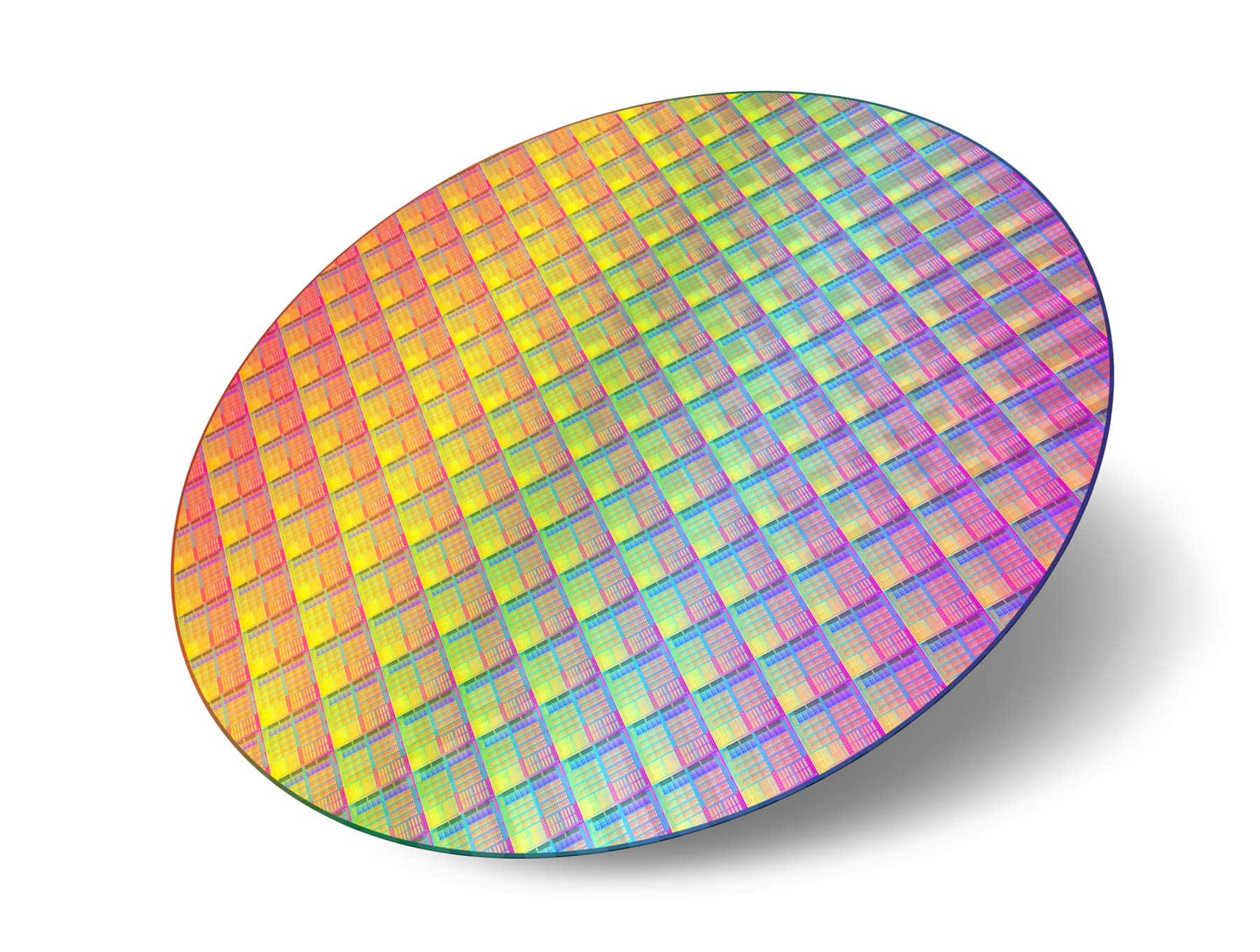
Integrated Circuit (IC) Packaging
Our waterjet technology is used for Integrated Circuit (IC) Packaging to cut multilayer materials made up of composite and copper layers. As packaging materials become more complex, it’s critical to produce clean cuts to avoid high process yield loss and warranty issues resulting from short outs. Unlike laser and wire saws, waterjet provides a clean cut that reduces smearing of copper and material delamination.
Waterjet cuts utilize shearing force; this results in a micro machining process that does not subject the material to high loads and minimizes the effects on the components of the IC package. Through this improved cutting process, our customers have experienced line yield improvements of up to 20%.
Waterjet is capable of cutting a very wide range of IC packages, reducing requirements for different types of machines for each packaging material.
Semiconductor Equipment Process Chamber Components
In the semiconductor wafer fabrication process, several different types of deposition methods are utilized to build-up different materials, like tungsten, titanium, and copper, onto the wafer.
These deposition processes include physical vapor deposition (PVD), chemical vapor deposition (CVD), electrochemical deposition (ECD), atomic layer deposition (ALD), among others. Inside the processing chamber, the components that hold the wafer during fabrication (shields, collimators, and disks, for example) experience product build-up. These deposits must be removed from the fabrication equipment during the component refurbishment process.
Our waterjet coating removal system enables reliable and cost-effective deposit removal. Ultrahigh-waterjet blasting is a preferred method for removing tough coatings with ease.

Coatings
Content Here

Underlying Components
Capacitor
Resistor
Transistors
Diodes

Texturing
Content Here
AREAS OF EXPERTISE:
Semiconductor & Chamber Components
Glass Applications
Microelectronics
Display Touchscreen Technology
Mobile Device Components & Assemblies
Ultrahigh-Pressure Waterjet Cutting
Our precision systems allow for high tolerance cutting of semiconductor chamber components such as pedestals, chucks, liners, disks, slots, base plates, chamber windows, and more.
Using our ultrahigh-pressure waterjet cutting solutions, we’re able to process advanced semiconductor materials including silicon, quartz, ceramics, stainless steel, and titanium.
Engineered-to-Order Solutions
In advanced industries like electronics, there are wide variations in product and, often, a need to fit new processes into existing production lines. We offer complete, total-care solutions: systems, automation, consumables, service, and support all from one trusted partner.